Samsung Electronics and SK Hynix are upgrading their China factories to make more advanced NAND flash, according to Reuters (Hyunjoo Jin, Liam Mo and Karen Freifeld, Oct. 21, 2026), which cites four people familiar with the plans. The stated aims are to counter Chinese rival YMTC and to meet AI demand.
Both companies confirmed that upgrades are underway and being done in close consultation with Washington, without giving details.
What each plant is said to be doing
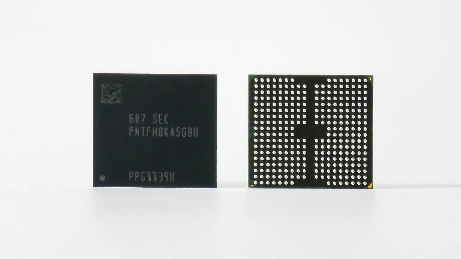
- Samsung, Xi'an: about 40% of Samsung's global NAND output. Now roughly 200 layers, reportedly converting to 286-layer V9 NAND (Samsung's ninth-generation NAND) under a project called "Monami". Reported targets are 5,000 wafers per month in December 2026 and 40,000 by December 2027. A wafer is the silicon disc chips are cut from, so this counts output.
- SK Hynix, Dalian: now 192 layers, looking to move to 240 or more. One source says SK Hynix is authorized to make up to 240 layers there and may seek US permission for R&D on 300-plus-layer chips. Dalian is the sole NAND site for Solidigm, the Intel NAND business SK Hynix bought in 2021.
Samsung said in a statement: "The company is not expanding production capacity or constructing new manufacturing facilities." It said the upgrade complies with US export regulations and aims to meet demand from global customers, including in the US.
Why export rules are the constraint
Layer count is how many layers of memory cells are stacked in a NAND chip. Outside China, Samsung sells up to 286 layers and showed a 400-plus-layer prototype in August, while SK Hynix sells up to 321.
US controls have limited some chipmaking equipment shipped to China since 2022. Both firms must apply for US licences each year to install US-made equipment, such as etching machines, in China.
The Commerce Department's Bureau of Industry and Security said in 2025 that it did not intend to grant licences to upgrade technology or expand capacity at these factories, and would consider applications to operate existing plants. BIS did not directly answer and referred to that 2025 statement.
Separately, a BIS final rule published Sept. 2, 2025 removed Samsung's and SK Hynix's China plants, and Intel's Dalian site, from the Validated End-User list, effective Dec. 31, 2025. The rule text does not address upgrades or capacity expansion.
The competitive picture
Omdia's second-quarter figures show YMTC at 38.5% of China NAND, up from 28% for all of 2025. Samsung is at 33.5%, down from 36%, and SK Hynix at 17%, down from 20%. YMTC makes 160- and 232-layer chips plus a small amount of 294-layer, and plans 300-plus.
Why it matters
Whether this eases memory tightness is not known. Samsung says it is not adding capacity, and it is not known how far US authorities have approved the licences these upgrades need.
Our earlier story reports that, per MoneyToday, Samsung is cutting Galaxy phone output as memory prices surge: see the Galaxy production cuts story. Samsung has not confirmed that. See also our Computing coverage.
Watch two things: the annual licence renewals, and whether Xi'an reaches the reported 5,000-wafer-per-month target in December 2026.